29/04/2024
Celebrations at April graduation


Since the announcement in 2004 by a pair of physicists at the University of Manchester that they had discovered a remarkable material a million times thinner than a human hair yet hundreds of time stronger than steel, graphene has been touted as a credible starting point for a wide range of technologies and applications. Those physicists, Andre Geim and Konstantin Novoselov, received the Nobel Prize in 2010 for their discovery. Wolfson’s Fellow Dr Antonio Lombardo has been working on graphene since 2008, exploring ways to turn the exceptional properties of this material into functional electronic devices.
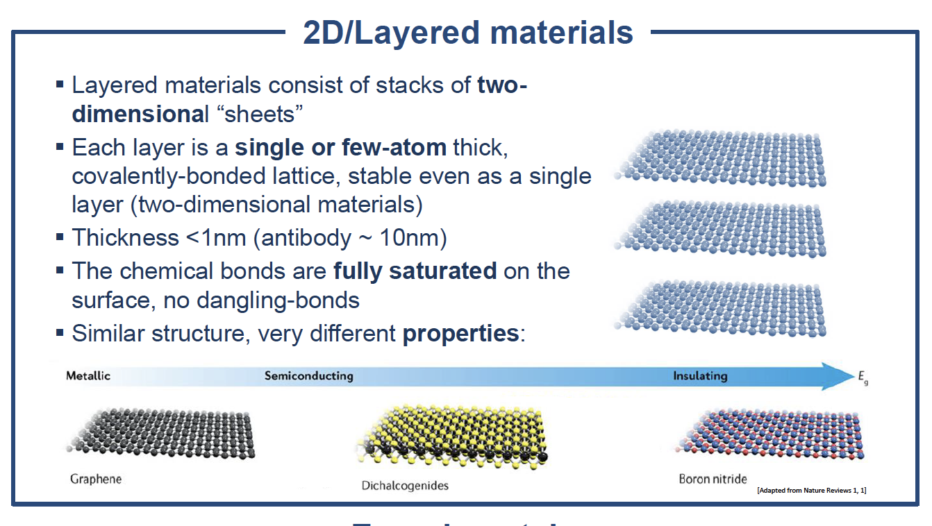
Graphene is the thinnest material known, a single layer of carbon atoms united in a two-dimensional hexagonal lattice. It is lightweight and flexible; it can bend, fold and stretch. It also has high electrical and heat conductivity – electrons in graphene move one hundred times faster than in silicon. It is the namesake of the Cambridge University institute where Antonio carries out his research, the Cambridge Graphene Centre (CGC).
Antonio, an electronic engineer, leads a small research group investigating new devices and technologies based on graphene and related materials.
“In fact, graphene is not the only material we work with,” says Antonio. “Over the last few decades we have developed a whole range of similar two-dimensional crystals with different properties. Some are insulators, others are semiconductors, conductors — even superconductors”
The mission of the GCG is to turn graphene and other two-dimensional materials into real technology, whether in electronics, photonics, energy storage, medicine, manufacturing, or communications. The remarkable properties of graphene make it ideal for a range of applications. However, widespread commercial uses remain in development whilst researchers work out the difficulties associated with producing it both in high quality and at high volumes.
In order to work with graphene, it must first be synthesized in sufficient quantities. Originally, it was produced by extracting single layers of carbon out of naturally occurring three-dimensional graphite.
“Nature produces excellent graphene but it is packed into its three-dimensional counterpart, graphite, and only small single-layer flakes can be extracted. We need larger areas for research and manufacturing. The progress in making synthetic graphene has been really impressive. We use a catalytic process known as chemical vapour deposition. You place a copper substrate and a hydrocarbon in a furnace and heat it to about 1000°C. When flowing on the copper the hydrocarbon molecules break, releasing the hydrogen. The carbon stays in a single atomic layer on the copper..”
Another option is to make a graphene dispersion, a solution of graphene flakes mixed with a solvent. This results in a type of ink that can be sprayed or printed or mixed with other materials. Graphene in this form is already being used in flexible printed electronics, photodetectors and biosensors.
Graphene stacks up
Antonio is particularly interested in heterostructures — combinations of these two-dimensional materials. Devices based on heterostructures are the backbone of several applications in photonics and electronics. However, the current technology is entirely based on just a few materials due to the need to match their lattice structures.
“The most interesting properties come when you have two or more materials and put them together to form heterostructures. Because the layered materials we work with have fully saturated surface bonds, you can arbitrarily stack them with no need for lattice matching, a bit like the pages of a book. The functionality of the devices you can make from these structures is based on the interface between the materials. For instance, graphene can be encapsulated in boron nitride, which is a good insulator, and protects the graphene from external factors which normally degrade its properties”.
But this introduces a problem: contamination from hydrocarbons, solvents, air, moisture or other impurities which result from the environment or manufacturing process can be trapped at the interface, forming blisters. The random placement of such blisters impedes the functioning of heterostructures and prevents the fabrication process from being scalable.
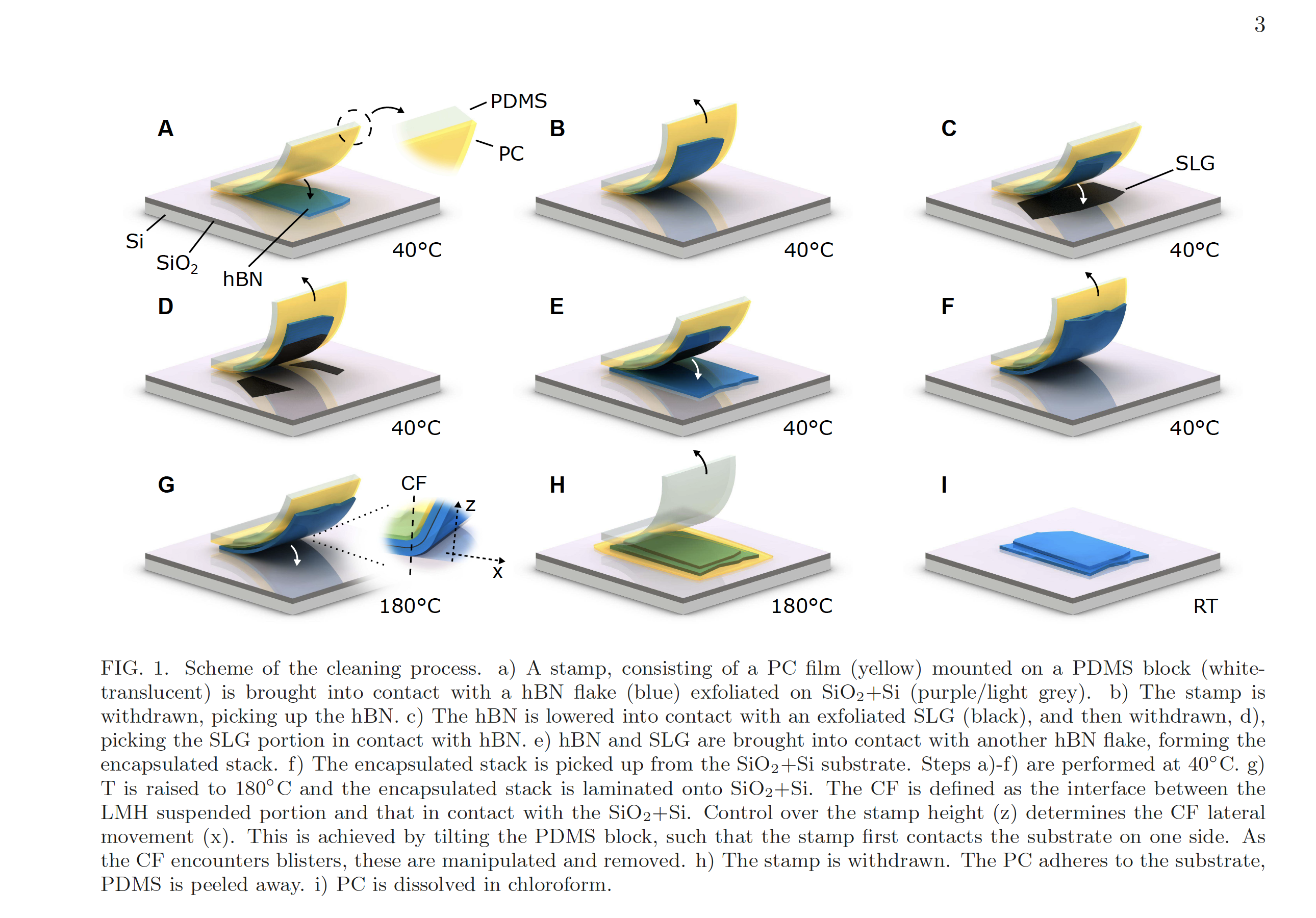
In a recently released paper published in Nature Communications, Cleaning interfaces in layered materials heterostructures, Antonio and his colleagues have demonstrated a new method of removing these contaminants. Essentially, they laminate the layered material heterostructure onto a substrate of silicon dioxide at a temperature of 180°C. This renders the blisters mobile enough that they can be mechanically pushed to the edges of the material and thus eliminated.
“The paper shows two new things: First, we can optimize the way we create heterostructures to have a clean interface across the whole structure. Second, this method is able to clean the interface even if it the materials are intentionally contaminated because we can remove the contaminations from fully-formed heterostructures.”
“The next step is to scale up the technology to make large wafers of a continuous layer of an insulator and graphene with the qualities you see in the paper. We are now applying the same approach to CVD-grown, large area graphene and boron nitride."
Making sensors of graphene
Another area of research Antonio is pursuing is the use of graphene in biosensors that work with microwaves to detect minute changes at a cellular or molecular level.
“Biological analytes interact quite strongly with microwaves. I am looking at the interaction between biological samples and microwaves at different frequencies to probe the properties of molecules and cells.”
Normally, this type of detection is done on a larger scale – at the level of tissues or organs – and Antonio would like to bring it down to the nanoscale, building devices of a size comparable to or smaller than a single cell. Also, unlike existing microwave sensors, the properties of the graphene itself can be directly modified by the proximity with the analyte, thus providing enhanced sensitivity.
Antonio has already demonstrated graphene microwave sensors capable of detecting specific sequences of DNA, but he plans to expand this approach to other biological materials.
“The long-term vision is to pack several sensors, each designed to detect a specific biological parameter, on the same chip. Working at this scale means that several analyses could be done from a single drop of analyte. Also, microwave technology is ubiquitous in communication and therefore such detectors could be easily incorporated into or interface with mobile devices such as phones.”